
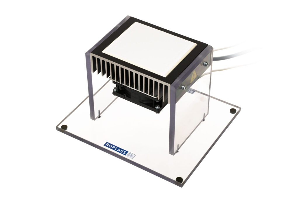
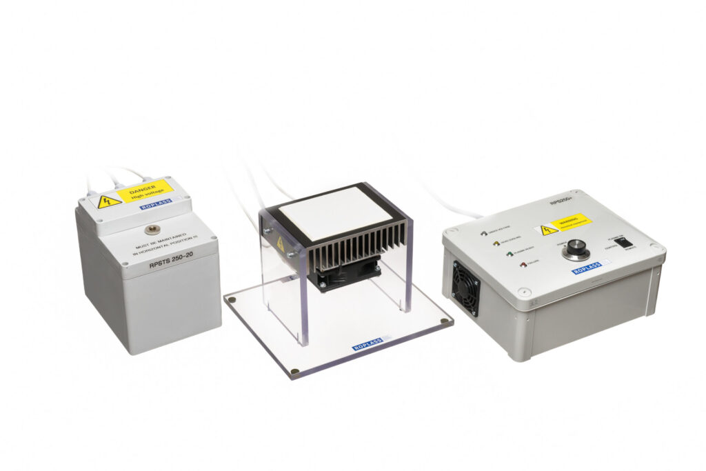
A 90 × 85 mm DCSBD source — no oil cooling required.
The RPS250+ is a compact DCSBD atmospheric-pressure plasma source (~90 × 85 mm treatment area, up to 250 W) engineered without oil-based cooling or insulation medium — significantly simplifying installation, handling and maintenance compared to larger DCSBD systems, while retaining the same noble-gas-free operation in ambient air.
The RPS250+ is designed for stable continuous operation in laboratory and industrial environments. In contrast to larger DCSBD systems such as the RPS400, the plasma unit itself does not require an oil-based cooling or insulation medium, significantly simplifying installation, handling, and maintenance. Plasma is generated directly in ambient air at atmospheric pressure, without the need for vacuum systems or external process gases.
The system enables fast and uniform surface activation, cleaning, and functionalisation through a dense, non-thermal plasma rich in reactive oxygen and nitrogen species (ROS/RNS), while preserving bulk material properties.
The RPS250+ is widely used for surface treatment of polymers, glass, ceramics, textiles, membranes, nanomaterial coatings, and other functional materials, as well as for laboratory testing and integration into automated and roll-to-roll processing lines.
Main features
- Power: 2× 230 V AC ±10 %, 50–60 Hz (separate supply for plasma generation and temperature control)
- Plasma parameters: up to 250 W sinusoidal high voltage (≈ 20 kV, 18–22 kHz) in one DCSBD plasma unit
- Plasma area: 90 mm × 85 mm
Gas: ambient air (open air operation; external process gases not required) - Operation mode: continuous operation
- Control: local control panel with external remote triggering (24 V DC)
- Scalability: modular DCSBD technology, suitable for integration into automated and roll-to-roll systems
Applications
- Laboratory and pilot-scale processing of flat, structured, and porous materials
- Surface activation, cleaning, and functionalisation, including controlled oxidation and reduction processes
- Treatment of various substrates, thin films, coatings, and nanomaterials
- Tailoring of surface electronic structure, including modification of optoelectronic properties, conductivity, band alignment, and effective bandgap